Microdevices Laboratory
Microdevice fabrication requires sophisticated equipment for the deposition, etching, and patterning of device layers, and must generally be done in a very clean environment to avoid defects and contamination. As a result, it is highly desirable to co-locate such activities, to allow expensive equipment to be shared, and to spread the maintenance burden over a larger base of activity.
While industrial “fabs” are usually designed for mass production of devices using a standard process, the MDL is much more flexible, allowing research, development, and small-scale production of a very broad range of devices. The MDL functions as a multi-user and shared equipment facility that is open to all JPL personnel; MDL access for users from outside institutions can also be arranged. The MDL Central Processing Group led by James Lamb is responsible for operational safety, facility maintenance, and installation and maintenance of shared-use equipment. This group is supported by MDL users through access fees and special equipment usage fees, and is also directly supported by JPL institutional funds.
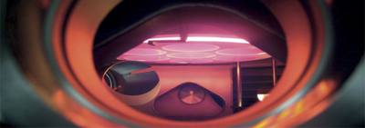
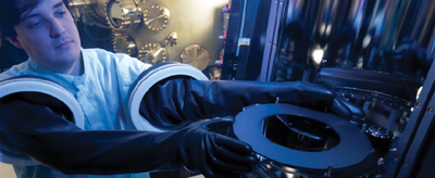
The heart of MDL is a 13,000-square-foot cleanroom that is used by over 70 research scientists. The MDL cleanroom is divided into various zones according to cleanliness standards, ranging from class 100,000 (ISO 8) for the rooms housing epitaxial deposition systems, to class 10 (ISO 4) for the lithography area. The MDL contains over 130 individual pieces of processing equipment, including systems for UV contact and projection lithography, electron-beam lithography, materials growth and deposition, wet and dry etching, thermal processing, and optical, structural, and electronic characterization. Much of the equipment is available to all MDL users on a shared basis; however, some equipment is dedicated to individual groups.
Personnel / Contacts:
- James Lamb - MDL Director
Ongoing Research Projects: